Mastering PCB Design with Eagle: A Comprehensive Guide
Introduction: Eagle, developed by Autodesk, is a widely-used electronic design automation (EDA) software suite for designing printed circuit boards (PCBs). From hobbyists to professional engineers, Eagle offers a powerful and intuitive platform for creating schematics, designing PCB layouts, and generating manufacturing files. In this extensive guide, we’ll explore the intricacies of designing PCBs in Eagle, covering everything from schematic capture to board layout and fabrication preparation.
Step 1: Installing Eagle and Getting Started Before diving into PCB design with Eagle, you’ll need to download and install the software on your computer. Eagle is available for Windows, macOS, and Linux platforms and can be obtained from the Autodesk website. Once installed, launch Eagle to begin your PCB design journey. Familiarize yourself with the Eagle user interface, including the control panel, project navigator, and schematic editor, where you’ll create and manage your PCB projects.
Step 2: Creating a New Project and Schematic The first step in designing a PCB in Eagle is to create a new project and schematic. A project in Eagle serves as a container for organizing related design files, such as schematics, layouts, and libraries. Use the “File” menu in Eagle to create a new project and schematic file, then start designing your circuit by placing components and connecting them with nets. Eagle provides a comprehensive library of electronic components, including resistors, capacitors, ICs, connectors, and more, which you can access from the component library.
Step 3: Placing Components and Wiring Nets Once you’ve created a schematic in Eagle, the next step is to place components and wire nets to define the connections between them. Use the component placement tools in Eagle to place components onto the schematic canvas and arrange them according to the desired circuit topology. Connect the components with nets by using the wire tool to draw connections between their pins. Eagle automatically assigns net names and labels to connected nets, making it easy to navigate and understand the schematic.
Step 4: Adding Value and Annotation After placing components and wiring nets in the schematic, it’s essential to add values and annotations to the components to provide additional information about their properties and functions. Values represent the nominal parameters of the components, such as resistance values for resistors and capacitance values for capacitors. Annotations assign unique reference designators to the components, such as R1, R2, C1, C2, etc., to distinguish them from each other. Use the value and annotation tools in Eagle to assign values and annotations automatically or manually as needed.
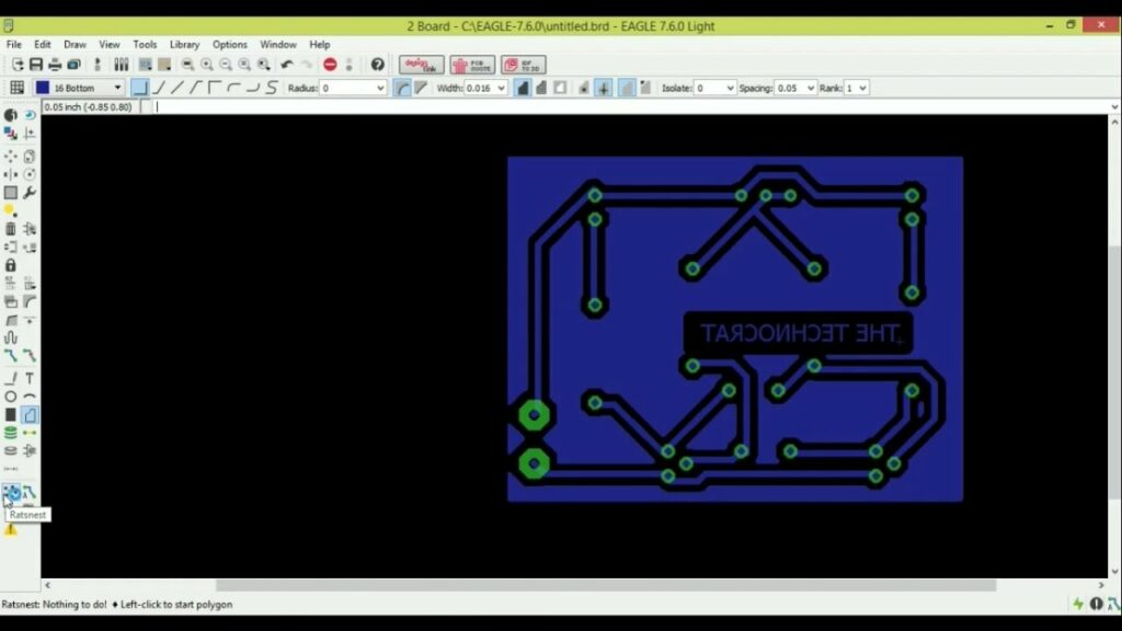
Step 5: Creating the PCB Layout With the schematic design complete, it’s time to create the PCB layout in Eagle. The PCB layout translates the schematic connections into physical traces and components on the PCB board. Use the “Switch to Board” command in Eagle to switch to the board layout editor, where you can arrange components, route traces, and define board dimensions. Eagle provides tools for placing components, routing traces, adjusting trace widths and clearances, and defining signal layers for routing.
Step 6: Routing Traces and Adding Copper Pour Once the components are placed on the PCB layout, the next step is to route traces to connect the component pins according to the schematic connections. Use the trace routing tools in Eagle to draw traces between component pads, vias, and other routing points. Eagle offers automatic and manual routing modes, allowing you to choose the most suitable routing strategy for your design. Additionally, you can add copper pour areas to the PCB layout to provide ground planes, power planes, or thermal management features.
Step 7: Design Rule Check (DRC) and Electrical Rule Check (ERC) Before finalizing the PCB layout, it’s crucial to perform a design rule check (DRC) and electrical rule check (ERC) to ensure that the design meets manufacturing and electrical specifications. The DRC checks for violations of design rules such as trace width, clearance, and spacing, while the ERC checks for electrical errors such as unconnected nets, short circuits, and design rule violations. Use the DRC and ERC tools in Eagle to identify and resolve any design issues before proceeding to fabrication.
Step 8: Generating Manufacturing Files Once the PCB layout is finalized and validated, it’s time to generate manufacturing files for fabrication. Manufacturing files include Gerber files, drill files, and assembly drawings, which provide the information necessary for fabricating and assembling the PCB. Use the CAM processor in Eagle to configure and generate the manufacturing files according to the requirements of your PCB manufacturer. Verify the generated files and review them thoroughly before sending them to the manufacturer for fabrication.
Conclusion: Designing PCBs in Eagle is a rewarding process that allows you to bring your electronic projects to life with precision and efficiency. By following the steps outlined in this comprehensive guide, you can leverage Eagle’s powerful features and capabilities to create schematics, design PCB layouts, and generate manufacturing files with confidence. Whether you’re a beginner or an experienced PCB designer, Eagle provides the tools you need to tackle the most challenging electronic design projects and turn your ideas into reality. With practice and experimentation, you can become proficient in designing PCBs in Eagle and unlock its full potential for realizing your electronic designs.